ASML Unveils EUV Breakthrough That Could Boost Chip Output by 50% by 2030
Daniel Okoye
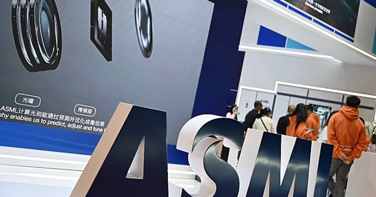
SAN DIEGO, Feb 23 (GeokHub) – Dutch semiconductor equipment leader ASML Holding has revealed a major technological advance in its extreme ultraviolet (EUV) lithography systems, a development that could increase chip production capacity by as much as 50% by the end of the decade.
- The breakthrough centers on enhancing the power of the EUV light source — the core component used to print advanced semiconductor chips. Company researchers say they have successfully raised light output to 1,000 watts, up from approximately 600 watts in current commercial systems.
Strengthening Technological Leadership
ASML remains the only commercial supplier of EUV lithography machines globally, providing critical manufacturing tools to leading chipmakers such as Taiwan Semiconductor Manufacturing Co and Intel. These machines are essential for producing advanced processors used in artificial intelligence, high-performance computing and next-generation electronics.
The EUV systems have become strategically important amid geopolitical tensions. U.S. administrations from both political parties have worked with Dutch authorities to restrict exports of the technology to China, prompting Beijing to accelerate domestic efforts to build competing systems.
Meanwhile, U.S.-based startups such as xLight are working to develop alternative EUV light sources, backed in part by government funding.
How the Breakthrough Works
EUV lithography relies on generating light with a wavelength of 13.5 nanometers. To achieve this, ASML machines fire a powerful carbon dioxide laser at microscopic droplets of molten tin, heating them into plasma hotter than the surface of the sun. This plasma emits EUV light, which is then collected and focused through precision optical systems supplied by Carl Zeiss AG to etch intricate circuit patterns onto silicon wafers.
The new advancement involves doubling the number of tin droplets fired per second to roughly 100,000 and refining the plasma formation process by using two shaping laser bursts instead of one. The result is a more stable and powerful EUV light source capable of significantly higher throughput.
Higher Output, Lower Cost
Greater EUV power reduces the exposure time required to print chips on each wafer. According to company projections, machines could process up to 330 wafers per hour by 2030, compared to around 220 wafers today.
Depending on chip design, a single wafer can contain dozens to thousands of individual chips. Faster wafer processing translates into lower per-chip production costs — a key factor as global demand for AI processors and advanced semiconductors continues to surge.
Researchers involved in laser technology describe the milestone as technically remarkable, noting that achieving sustained one-kilowatt EUV output under production conditions is a significant engineering accomplishment.
ASML executives also indicated that the 1,000-watt achievement may not represent the ceiling. The company sees a pathway toward 1,500 watts and potentially even 2,000 watts in future generations of the technology.